 Global - English
 Spanish - Español
 French - Français
 Russian - Pусский язык
 Chinese - 中文
 Korean - 한국어
 Vietnamese - Tiếng Việt
Do You Know about the UC284× Working Status?
About how UC284× works, it involves knowledge about analog and digital. So today, let the author lead you to understand it. I hope that you will gain something after reading it.
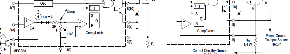
Figure 1 is a representative block diagram of UC284×. Since each peripheral condition may affect the output, we try to push forward from the output. According to the conditions of the switch tube being turned on and off, the corresponding input relationship is sequentially pushed out.
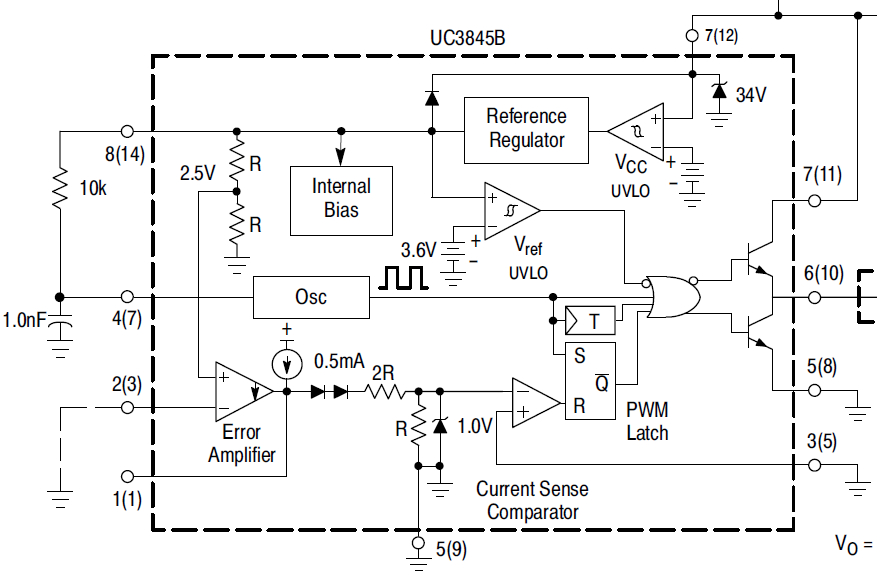
Representative block diagram of UC284×
First analyze the driven output circuit. Looking at Figure 2, the drive output consists of an OR gate and a push-pull circuit. When the switch is turned off, the push-pull output is low, or the gate inverting output is low, and the non-inverting output is high. At this time, the OR input has a high level. Note that as long as the OR input is high, the switch must be turned off, otherwise the switch is turned on, and the conditions are quite simple.
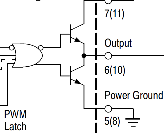
Analyze the driven output circuit
Then analyze the input of the OR gate. The input of the OR gate includes: 1. Reference under voltage lockout; 2. Oscillator output; 3. PWM latch output. Under what state do they have a high level (switching off)?
Analyze the input of the OR gate
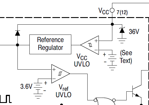
Figure 3 shows the output of the reference undervoltage lockout section. When the power supply voltage of UC284× is lower than the power supply undervoltage lockout value (the upper and lower thresholds of the VCC comparator are: UC2844 16V/10V; UC2845 8.4V/7.6V). That is, the reference and regulator output is lower than 3.6V, the reference undervoltage lockout outputs a low level, and is inverted after being inverted. What does it mean? Indicates that the output is not allowed when the power supply voltage is insufficient. The reference undervoltage lockout does not contribute to the output of the UC284× when the circuit is operating normally.
The output of the reference undervoltage lockout section
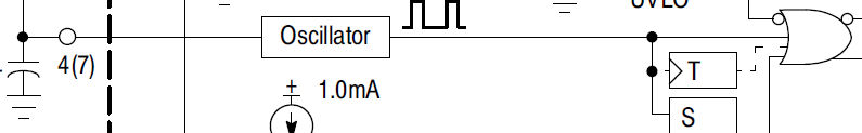
Figure 4 shows the oscillator output. When the timing capacitor is charged, the oscillator outputs a low potential; when the timing capacitor is discharged, the oscillator outputs a high potential (the above principle is fully explained in the UC284× specification). The above understanding is that the switching transistor is allowed to conduct when the timing capacitor is charged, and the switching tube is not allowed to be turned on when the timing capacitor is discharged.
The oscillator output
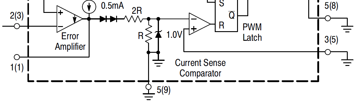
Figure 5 shows the PWM latch. When the oscillator outputs a high level, the PWM latch is set and its inverting output is low. When the current sense comparator outputs a high level, the PWM latch is cleared and its inverted output is high. When the error amplifier sends the voltage to the current detection comparator input terminal (-) is greater than the current feedback voltage, the current detection comparator outputs a low level, and the output of the UC284× is high in the normal state, allowing the switch to be turned on. When the error amplifier sends the voltage to the current detection comparator input terminal (-) less than the current feedback voltage, the current detection comparator outputs a high level, the PWM latch is cleared, and its inverting output is low. The output of the UC284× is low in the normal state, and the switch is turned off.
At present, it is found that there are errors in the in-phase and inverting terminals of the current detecting comparator on the product specification, as shown in FIG. 6. Actually, the error amplifier should be sent to the current detection comparator input terminal as the inverting terminal, and the current feedback voltage to the current detection comparator input terminal as the non-inverting terminal.
There are errors in the in-phase and inverting terminals of the current detecting comparator
In summary:
1. When the power supply voltage is under voltage, the switch tube is not allowed to conduct. When the voltage is normal, the switching tube is not affected by the power supply voltage.
2. When the timing capacitor is charged, the switch tube is allowed to conduct. When the timing capacitor is discharged, the switch tube is not allowed to conduct.
3. When the voltage sent by the error amplifier to the input (-) of the current sense comparator is greater than the current feedback voltage, the switch is allowed to conduct. When the error amplifier sends a voltage to the current sense comparator input (-) that is less than the current feedback voltage, the switch is turned off.